Sun Feb 12, 2012
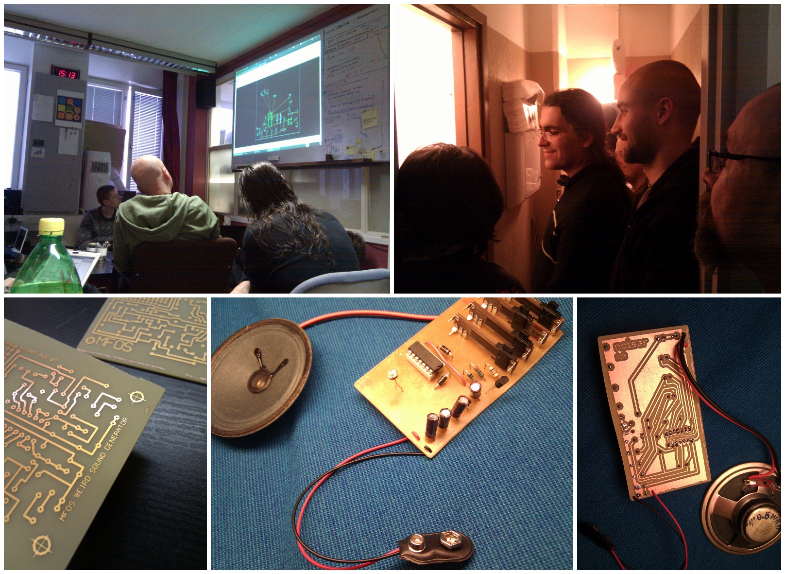
I spent last Saturday building a Noiser 1.0 at Hacklab Helsinki. It was a long process:
- + A software called Eagle was used to design a circuit board. All the components were laid out in this design program.
+ Later the components were moved around optimizing the board shape.
+ When the design was good enough we printed a black and white image on a transparency using a laser printer.
+ Shining ultraviolet light for 125 seconds through the transparency, the shape was transferred to a board.
+ The board was put into some liquid for 15 seconds. We wore protective glasses and gloves.
+ The board was rinsed with water, and submerged in another liquid for half hour. You can see the result in the bottom left photo.
+ We then drilled lots of holes through the board.
+ We placed all the components on the board, with the legs going through those little holes.
+ The components were soldered onto the board.
+ We finally connected the battery and you can see what happened on this video.
I will definitely create more boards. And I’m really looking forward to using the 3D printer to create some interesting shapes.